|
Datenblatt-Suchmaschine für elektronische Bauteile |
|
|
Datenblatt-Suchmaschine für elektronische Bauteile |
|
MCP3912 Datenblatt(PDF) 32 Page - Microchip Technology |
|
|
|||||||||||||||||||||||||||||
MCP3912 Datenblatt(HTML) 32 Page - Microchip Technology |
|
|
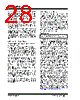
32 / 82 page  MCP3912 DS20005348A-page 32 2014 Microchip Technology Inc. 5.3.4 DITHER SETTINGS All modulators include a dithering algorithm that can be enabled through the DITHER<1:0> bits in the Configuration register. This dithering process improves THD and SFDR (for high OSR settings), while slightly increasing the noise floor of the ADCs. For power metering applications and applications that are distortion sensitive, it is recommended to keep DITHER at maximum settings for best THD and SFDR performance. In the case of power metering applications, THD and SFDR are critical specifications. Optimizing SNR (noise floor) is not problematic due to the large averaging factor at the output of the ADCs. Therefore, even for low OSR settings, the dithering algorithm will show a positive impact on the performance of the application. 5.4 SINC3 + SINC1 Filter The decimation filter present in all channels of the MCP3912 is a cascade of two sinc filters (sinc3+sinc1): a third-order sinc filter with a decimation ratio of OSR3, followed by a first-order sinc filter with a decimation ratio of OSR1 (moving average of OSR1 values). Figure 5-2 represents the decimation filter architecture. FIGURE 5-2: MCP3912 Decimation Filter Block Diagram. Equation 5-1 calculates the filter z-domain transfer function. EQUATION 5-1: SINC FILTER TRANSFER FUNCTION Equation 5-2 calculates the settling time of the ADC as a function of DMCLK periods. EQUATION 5-2: The SINC1 filter following the SINC3 filter is only enabled for the high OSR settings (OSR > 512). This SINC1 filter provides additional rejection at a low cost with little modification to the -3 dB bandwidth. The resolution (number of possible output codes expressed in powers of two or in bits) of the digital filter is 24-bit maximum for any OSR and data format choice. The resolution depends only on the OSR<2:0> settings in the CONFIG0 register per the Table 5-3. Once the OSR is chosen, the resolution is fixed and the output code respects the data format defined by the WIDTH_DATA<1:0> setting in the STATUSCOM register (see Section 5.5 “ADC Output Coding”). Modulator Output SINC 3 SINC 1 Decimation Filter Output OSR3 OSR1 4 16 (WIDTH=0) 24 (WIDTH=1) Decimation Filter OSR1=1 Hz 1z - OSR 3 – 3 OSR 3 1z 1 – – 3 ---------------------------------------------- 1z - OSR 1 OSR 3 – OSR 1 1z - OSR 3 – --------------------------------------------------------- = Where z EXP 2 jf in DMCLK = Sett lingTi me DMCLKperiods 3OSR 3 OSR 1 1 – OSR 3 + = |
|
Link URL |
| War ALLDATASHEET hilfreich? [ DONATE ] |
Über Alldatasheet | Werbung | Kontakt | Privatsphäre und Datenschutz | Link zum Datenblatt | Linktausch | Hersteller All Rights Reserved©Alldatasheet.com |
| Russian : Alldatasheetru.com | Korean : Alldatasheet.co.kr | Spanish : Alldatasheet.es | French : Alldatasheet.fr | Italian : Alldatasheetit.com Portuguese : Alldatasheetpt.com | Polish : Alldatasheet.pl | Vietnamese : Alldatasheet.vn Indian : Alldatasheet.in | Mexican : Alldatasheet.com.mx | British : Alldatasheet.co.uk | New Zealand : Alldatasheet.co.nz |
|
Family Site : ic2ic.com |
icmetro.com |
 German ▼
 English
 Chinese
 German
 Japanese
 Russian
 Korean
 Spanish
 French
 Italian
 Portuguese
 Polish
 Vietnamese
 Indian
 Mexican
 British
 New Zealand