|
Datenblatt-Suchmaschine für elektronische Bauteile |
|
|
Datenblatt-Suchmaschine für elektronische Bauteile |
|
MCP3912 Datenblatt(PDF) 53 Page - Microchip Technology |
|
|
|||||||||||||||||||||||||||||
MCP3912 Datenblatt(HTML) 53 Page - Microchip Technology |
|
|
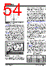
53 / 82 page  2014 Microchip Technology Inc. DS20005348A-page 53 MCP3912 7.2 Power Supply Design and Bypassing The MCP3912 device was designed to measure posi- tive and negative voltages that might be generated by a current sensing device. This current sensing device, with a common mode voltage close to 0V, is referred to as AGND, which is a shunt or current transformer (CT) with burden resistors attached to ground. The high per- formance and good flexibility that characterize this ADC enables them to be used in other applications, as long as the absolute voltage on each pin, referred to AGND, stays in the -1V to +1V interval. In any system, the analog ICs (such as references or operational amplifiers) are always connected to the analog ground plane. The MCP3912 should also be considered as a sensitive analog component, and con- nected to the analog ground plane. The ADC features two pairs of pins: AGND, AVDD, DGND and DVDD. For best performance, it is recommended to keep the two pairs connected to two different networks (Figure 7-2). This way, the design will feature two ground traces and two power supplies (Figure 7-3). This means the analog circuitry (including MCP3912) and the digital circuitry (MCU) should have separate power supplies and return paths to the external ground reference, as described in Figure 7-2. An example of a typical power supply circuit, with different lines for ana- log and digital power, is shown in Figure 7-3. A possible split example is shown in Figure 7-4, where the ground star connection can be done at the bottom of the device with the exposed pad. The split here between analog and digital can be done under the device, and AVDD and DVDD can be connected together with lines coming under the ground plane. Another possibility, sometimes easier to implement in terms of PCB layout, is to consider the MCP3912 as an analog component and, therefore, connect both AVDD and DVDD together, and AGND and DGND together with a star connection. In this scheme, the decoupling capacitors may be larger due to the ripple on the digital power supply (caused by the digital filters and the SPI interface of the MCP3912) now causing glitches on the analog power supply. FIGURE 7-2: All Analog and Digital Return Paths Need to Stay Separate with Proper Bypass Capacitors. FIGURE 7-3: Power Supply with Separate Lines for Analog and Digital Sections. Note the "Net Tie" Object NT2 that Represents the Start Ground Connection. VA VD MCU “Star” Point IA ID ID IA AVDD DVDD AGND DGND D-= A-= 0.1 μF MCP39XX 0.1 μF C |
|
Link URL |
| War ALLDATASHEET hilfreich? [ DONATE ] |
Über Alldatasheet | Werbung | Kontakt | Privatsphäre und Datenschutz | Link zum Datenblatt | Linktausch | Hersteller All Rights Reserved©Alldatasheet.com |
| Russian : Alldatasheetru.com | Korean : Alldatasheet.co.kr | Spanish : Alldatasheet.es | French : Alldatasheet.fr | Italian : Alldatasheetit.com Portuguese : Alldatasheetpt.com | Polish : Alldatasheet.pl | Vietnamese : Alldatasheet.vn Indian : Alldatasheet.in | Mexican : Alldatasheet.com.mx | British : Alldatasheet.co.uk | New Zealand : Alldatasheet.co.nz |
|
Family Site : ic2ic.com |
icmetro.com |
 German ▼
 English
 Chinese
 German
 Japanese
 Russian
 Korean
 Spanish
 French
 Italian
 Portuguese
 Polish
 Vietnamese
 Indian
 Mexican
 British
 New Zealand