|
Datenblatt-Suchmaschine für elektronische Bauteile |
|
|
Datenblatt-Suchmaschine für elektronische Bauteile |
|
MCP3912 Datenblatt(PDF) 46 Page - Microchip Technology |
|
|
|||||||||||||||||||||||||||||
MCP3912 Datenblatt(HTML) 46 Page - Microchip Technology |
|
|
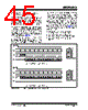
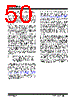
46 / 82 page  MCP3912 DS20005348A-page 46 2014 Microchip Technology Inc. 6.5.1 CONTINUOUS READ The STATUSCOM register contains the read communica- tion loop settings for the internal register address pointer (READ<1:0> bits). For Continuous Read modes, the address selection can take the following four values: Any SDI data coming after the control byte is not considered during a continuous read communication. The following figures represent a typical continuous read communication on all four ADC channels in TYPES mode with the default settings (DR_LINK = 1, READ<1:0> = 10, WIDTH_DATA<1:0> = 01) in case of the SPI Mode 0,0 (Figure 6-7) and SPI Mode 1,1 (Figure 6-8). In SPI Mode (1,1), the SDO pin stays in the last state (LSB of previous data) after a complete reading which also allows seamless continuous Read mode (see Figure 6-8). FIGURE 6-7: Typical Continuous Read Communication (WIDTH_DATA<1:0> = 01, SPI Mode 0,0). FIGURE 6-8: Typical Continuous Read Communication (WIDTH_DATA<1:0> = 01, SPI Mode 1,1). TABLE 6-1: ADDRESS SELECTION IN CONTINUOUS READ READ<1:0> Register Address Set Grouping for Continuous Read Communications 00 Static (no incrementation) 01 Groups 10 Types (default) 11 Full Register Map Note: For continuous reading of ADC data in SPI Mode 0,0 (see Figure 6-7), once the data has been completely read after a data ready, the SDO pin will take the MSB value of the previous data at the end of the reading (falling edge of the last SCK clock). If SCK stays idle at logic low (by definition of Mode 0,0), the SDO pin will be updated at the falling edge of the next data ready pulse (synchronously with the DR pin falling edge with an output timing of tDODR) with the new MSB of the data corresponding to the data ready pulse. This mechanism allows the MCP3912 to continuously read ADC data outputs seamlessly, even in SPI Mode (0,0). Don’t care SCK SDI SDO CS Hi-Z 8x 0x01 24x DATA_CH0 ... DATA_CH Starts read sequence at address00000 Complete READ sequence on ADC outputs channels 0 to DATA_CH1 24x ... 24x 24x DATA_CH0 ... DATA_CH1 24x ... 24x DATA_CH Don’t care DR DATA_CH0<23> New data DATA_CH0<23> Old data Complete READ sequence on new ADC outputs channels 0 to Don’t care SCK SDI SDO CS Hi-Z 8x 0x01 24x DATA_CH0 ... DATA_CH Starts read sequence at address 00000 Complete READ sequence on ADC outputs channels 0 to DATA_CH1 24x ... 24x 24x DATA_CH0 ... DATA_CH1 24x ... 24x DATA_CH Don’t care DR Complete READ sequence on new ADC outputs, channels 0 to Stays at DATA_CH <0> |
|
Link URL |
| War ALLDATASHEET hilfreich? [ DONATE ] |
Über Alldatasheet | Werbung | Kontakt | Privatsphäre und Datenschutz | Link zum Datenblatt | Linktausch | Hersteller All Rights Reserved©Alldatasheet.com |
| Russian : Alldatasheetru.com | Korean : Alldatasheet.co.kr | Spanish : Alldatasheet.es | French : Alldatasheet.fr | Italian : Alldatasheetit.com Portuguese : Alldatasheetpt.com | Polish : Alldatasheet.pl | Vietnamese : Alldatasheet.vn Indian : Alldatasheet.in | Mexican : Alldatasheet.com.mx | British : Alldatasheet.co.uk | New Zealand : Alldatasheet.co.nz |
|
Family Site : ic2ic.com |
icmetro.com |
 German ▼
 English
 Chinese
 German
 Japanese
 Russian
 Korean
 Spanish
 French
 Italian
 Portuguese
 Polish
 Vietnamese
 Indian
 Mexican
 British
 New Zealand